
Direct Laser Writing
Rapid prototyping
To fabricate three-dimensional photonic-crystal and metamaterial structures, we have developed and optimized a technique called direct laser writing (DLW). In DLW, femtosecond pulses are very tightly focused to a diffraction-limited optical spot. Only in the central region, the light intensity is sufficiently large to lead to significant two-photon absorption. Hence, for a negative-tone photoresist, only this central three-dimensional volume element or “voxel” (in analogy to the two-dimensional pixel element “pixel”) remains after the development process. Using computer controlled piezoelectric scanning stages, essentially any arbitrary complex three-dimensional nanostructure can be fabricated along these lines. An early example has been a three-dimensional face-centered-cubic woodpile photonic crystal with a stop band at telecommunication wavelengths. In 2007, we have commercialized the DLW technology via the start-up company Nanoscribe GmbH. Typically, lateral feature sizes as small as 80 nm can be achieved with 800 nm fundamental DLW laser wavelength.
Beyond the diffraction limit
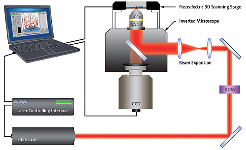
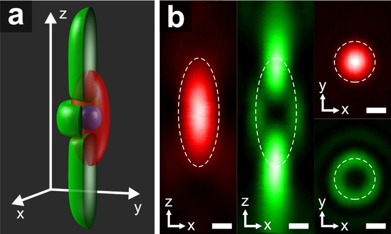
Nevertheless, regular DLW has been limited by the Abbe diffraction barrier. With respect to optical microscopy, Abbe’s law states that one cannot resolve a grating the period of which is much smaller than half the wavelength of light. The corresponding limitation for optical lithography can be circumvented by incorporating a trick known from optical fluorescence microscopy called stimulated emission depletion (STED). In essence, the width of a fat line can be reduced by erasing its edges. To implement STED-inspired DLW optical lithography, special home-made photoresists are essential. On this basis, our group has recently succeeded in breaking the lateral as well as the axial Abbe barrier for what we believe to be the first time. This technology has, e.g., enabled the first polarization-independent three-dimensional invisibility cloak at visible wavelengths in our group and is presently used for fabricating photonic metamaterials and visible-wavelength three-dimensional photonic-band-gap materials. In collaboration with chemists, we are also developing further novel photoresists, aiming at achieving spatial resolutions of just some tens of nanometers. This would approach the ultimate dream of nanoscience, namely to shape and control matter in three dimensions from the atomic to the macroscopic scale.
A complete list of publications can be found here.